Improving the performance of thermoelectric materials by microstructure design
Ecological concerns drive the exploration of “green” alternatives to generate electricity. One environmentally-friendly approach is to recycle waste heat by thermoelectric devices to realize the heat-to-electricity conversion. These devices are without moving parts, noise- and carbon-emission free, and can be miniaturized and combined with other energy conversion technologies such as direct solar thermal energy conversion.
Ecological concerns drive the exploration of “green” alternatives to generate electricity. One environmentally-friendly approach is to recycle waste heat by thermoelectric devices to realize the heat-to-electricity conversion. These devices are without moving parts, noise- and carbon-emission free, and can be miniaturized and combined with other energy conversion technologies such as direct solar thermal energy conversion. Their conversion efficiency is defined by a dimensionless figure of merit ZT, which relates the electrical conductivity σ, the Seebeck coefficient S, the temperature T, and the thermal conductivity κ as follows: ZT=S2σ∙Tκ . Substantial research & industrial efforts are pursued to optimize the thermoelectric performance by doping and isoelectronic alloying, i.e. tuning the alloy’s composition. However, the role of microstructure, and the interaction of dopants with lattice imperfections, are rarely considered and studied, which limits the opportunity for science-driven optimization of the material.
Our interdepartmental activities aim to address this knowledge gap by characterizing the multiscale complexity of the microstructure of a range of thermoelectric materials including half- and full-Heuslers [1, 2], AgSbTe2 [3], and PbTe [4] and correlating it with their thermal and electrical conductivity. This will ultimately enable us to develop thermoelectric materials by microstructure design.
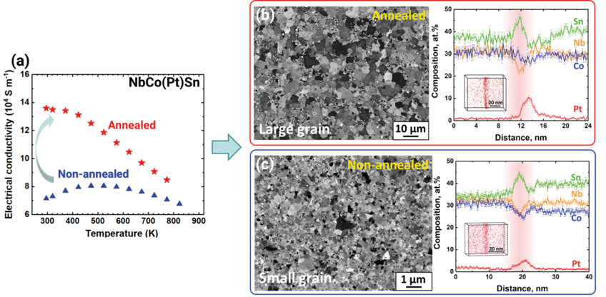
We will showcase our approach here with results on Half-Heusler (HH) compounds, with a stoichiometry NbCoSn, that stand out as state-of-the-art thermoelectric materials for medium-to-high temperature applications. We studied Pt-doped NbCoSn as part of a collaboration with C. Felser (Max Planck Institute for Chemical Physics of Solids). Pt substitutes Co, thereby providing an additional electron, making it an effective dopant. Pt-doping leads to significant improvements in the electrical power factor and reduces lattice thermal conductivity, as reported for NbCo1-xPtxSn (x=0.00-0.15) [5]. Interestingly in this series, the sample with x=0.05 (annealed, NbCoSn-Pt-AN) exhibits a striking increase in electrical conductivity compared to x=0.06 (non-annealed, NbCoSn-Pt), as shown in Fig. 1(a).

Grain size. The stored deformation energy induced by ball-milling drives grain growth during the post-sintering annealing. It leads to a tenfold increase in grain size (0.23 ± 0.12 μm to 2.38 ± 1.65 μm) and thus a largely reduced grain boundary (GB) area of NbCoSn-Pt-AN, as revealed by backscattered electron imaging in a scanning electron microscope (SEM) (Fig. 1b and c). The difference in grain size between the two samples becomes the first key microstructural factor influencing the electrical conductivity through grain boundary scattering.
Grain boundary segregation. Atom probe tomography shows that the intragranular Pt-content is similar for both alloys, i.e. ~1.35 ± 0.09 at.% for NbCoSn-Pt and 1.27 ± 0.09 at.% for NbCoSn-Pt-AN. The improvement in electrical conductivity does hence not arise from the doping level, rather, from the microstructure evolution. Pt-segregation to GBs is found in both samples Fig.1 (b) and (c), with varying degree of Pt enrichment across different GBs, likely depending on their geometric characteristics.
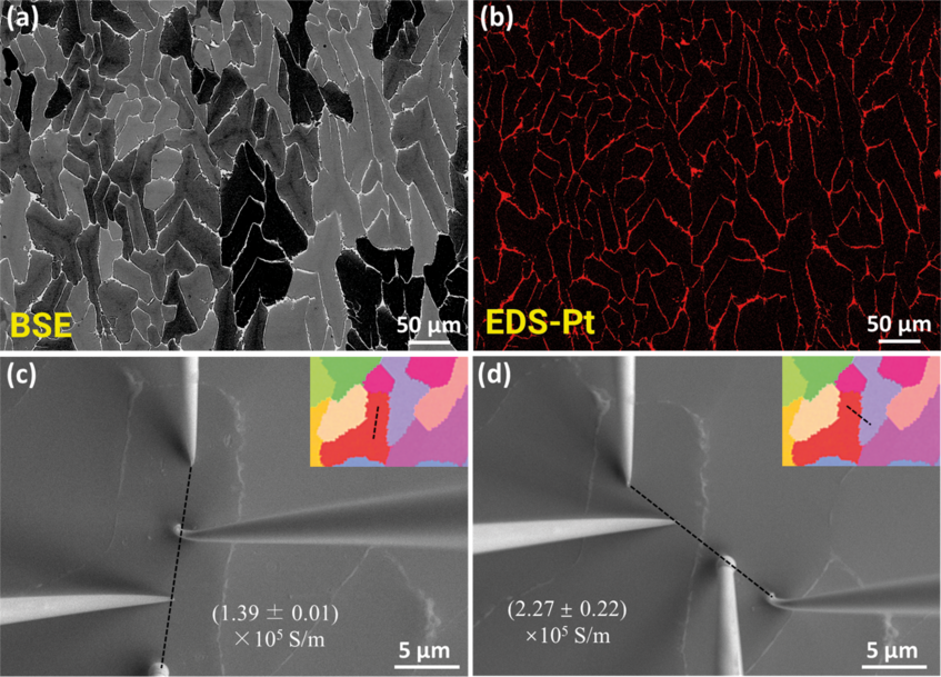
Local electrical conductivity. To assess the impact of this GBs segregation of Pt on the electrical conductivity, we used an in situ four-point-probe technique within an SEM to measure the local electrical conductivity [6]. As the grain size must be sufficiently large to separate the four probes, we selected the NbCoSn-Pt (x=0.05) sample before ball milling with an average grain size of approx. 25 μm. The corresponding backscattered electron micrograph and compositional map from energy-dispersive X-ray spectroscopy for Pt are respectively shown in Fig. 2 (a) and (b), highlighting Pt enrichment and percolation along grain boundaries. The electrical conductivity was measured inside two adjacent grains and across the corresponding high angle grain boundary, as assessed by electron-backscattered diffraction (inset in Fig. 2c and d). One example of the position layout of the four probes is displayed in Fig. 2(c) for grain interior and Fig. 2(d) for a high angle grain boundary. The absolute value of the electrical conductivity is (1.39 ± 0.01) ×105 S/m for the grain interior, i.e. comparable with the value of NbCoSn-Pt-AN at room temperature. Across the GB, and despite possible space-charge effects, the conductivity increases almost twofold to (2.27 ± 0.22) ×105 S/m thanks to the enrichment of Pt at GBs. We therefore prove the beneficial effect of GB-segregation on the electrical conductivity. It is hence possible to use grain boundary engineering to manipulate the GB-transport properties, opening new possibilities for optimizing TE performance.

Generalization. The philosophy and approach that was discussed here was deployed to analyze several other materials, for instance, PbTe and AgSbTe2, Ti(Co, Fe)Sb Half-Heusler with the collaboration with G. J. Snyder (Northwestern University, USA), and the Fe2AlV full-Heusler alloy that is being synthesized in-house. For the Fe2AlV, we also investigated the possibilities of using the selective-laser melting machine to manipulate the microstructure by surface-laser remelting [7], which can be seen as a precursor to additive manufacturing. We demonstrated an influence of grain boundary and structural defects on both electrical and thermal conductivities measured locally. We are also exploring the overlooked effect of impurity introduction during processing for instance.
1. Gomell, L.; Roscher, M.; Bishara, H.; Jägle, E.A.; Scheu, C.; Gault, B.: Scr. Mater. 193 (2021) 153.
2. Luo, T.; Serrano-Sánchez, F.; Bishara, H.; Zhang, S.; Bueno Villoro, R.; Kuo, J.J.; Felser, C.; Scheu, C.; Snyder, G.J.; Best, J.P.; Dehm, G.; Yu, Y.; Raabe, D.; Fu, C.; Gault, B.: Acta Mater. 217 (2021) 117147.
3. Abdellaoui, L.; Zhang, S.; Zaefferer, S.; Bueno-Villoro, R.; Baranovskiy, A.; Cojocaru-Mirédin, O.; Yu, Y.; Amouyal, Y.; Raabe, D.; Snyder, G.J.; Scheu, C.: Acta Mater. 178 (2019) 135.
4. Abdellaoui, L.; Chen, Z.; Yu, Y.; Luo, T.; Hanus, R.; Schwarz, T.; Bueno Villoro, R.; Cojocaru-Mirédin, O.; Snyder, G.J.; Raabe, D.; Pei, Y.; Scheu, C.; Zhang, S.: Adv. Funct. Mater. (2021) 2101214.
5. Serrano-Sánchez, F.; Luo, T.; Yu, J.; Xie, W.; Le, C.; Auffermann, G.; Weidenkaff, A.; Zhu, T.; Zhao, X.B.; Alonso, J.A.; Gault, B.; Felser, C.; Fu, C.: J. Mater. Chem. A 6 (2020) 4883.
6. Bishara, H.; Ghidelli, M.; Dehm, G.: ACS Appl. Electron. Mater. 2(7) (2020) 2049.
7. Gomell, L.; Haeger, T.; Roscher, M.; Bishara, H.; Heiderhoff, R.; Riedl, T.; Scheu, C.; Gault, B.: arXiv preprint arXiv:2107.07327. (2021).
