Seeing how grain boundaries transform
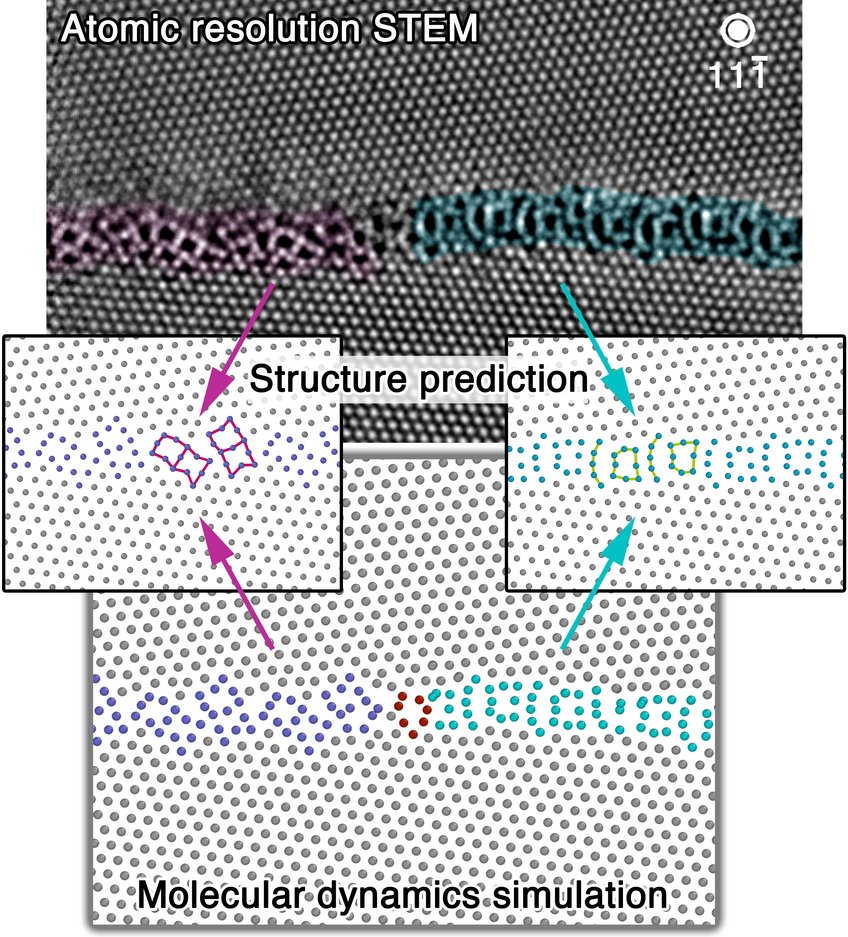
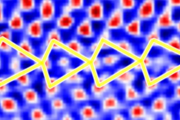
The key to experimentally observe transforming grain boundaries was to utilize atomic resolution microscopy. The grain boundaries were studied in thin films of pure copper particularly by aberration-corrected STEM. Our results clearly show that two grain boundary structures coexist with different atomic arrangements (see Fig. 1). However, the grain boundary plane orientation, crystallite misorientation and chemical composition does not change. The grain boundary phases can be described as motifs with pearl (green) and domino-shaped (purple) structure and they were modelled using a novel grain boundary structure search algorithm (see Fig. 1), which is capable of finding the experimentally observed structures (Dr. Timofey Frolov, Lawrence Livermore National Laboratory). Moreover, finite-temperature molecular dynamics simulations explored their transformation kinetics (see Fig. 1). The predicted structures not only perfectly resemble the experimental observations, but demonstrate that the grain boundary phases can transform into each other by changing temperature or stress. Additionally, the simulations indicate that the grain boundary phase junction, a novel line defect, which has not been considered previously, is rate controlling. Furthermore, the grain boundary phases are characterized by different properties, which determine how the interface phases move, how they take up impurity elements or how they mechanically deform. Through these observations we have to re-think how interfaces behave while exposing a material to temperature and/or stress. Understanding how grain boundaries transform provides a new view on still unexplained material phenomena, such as abnormal grain growth, and paves new ways to consider interface transitions as a material design element. The different states of grain boundaries or interfaces can have a strong impact on the corrosion behaviour of materials, how they behave under catalytic conditions or even play an important role in the failure of microelectronic devices. We aim to widen the current observations to experiments done at different temperatures, under stress and in the presence of impurities to establish a complete understanding of these phase transformations, thus being able to design material properties by reaching out to a holistic grain boundary engineering.

Figure 1: Atomic resolution scanning transmission electron microscopy (STEM) image of a grain boundary phase transformation in elemental copper. The corresponding grain boundary phases are predicted by grain boundary structure search. The dynamics of the grain boundary phase transformation as observed in experiment is modelled by molecular dynamics simulations.


