III-V Semiconductors and alloys at the nanoscale: materials design for novel optoelectronic and elastic properties
Designing and controlling the nanoscale structure of semiconductors and alloys is a promising strategy in order to create materials with targeted optoelectronic and mechanical properties. In this context, III-V and III-N nanostructures are particularly attractive candidates for surmounting materials-related challenges in applications ranging from optoelectronics, power electronics and hydrogen diffusion barriers to hard and wear resistant coatings.
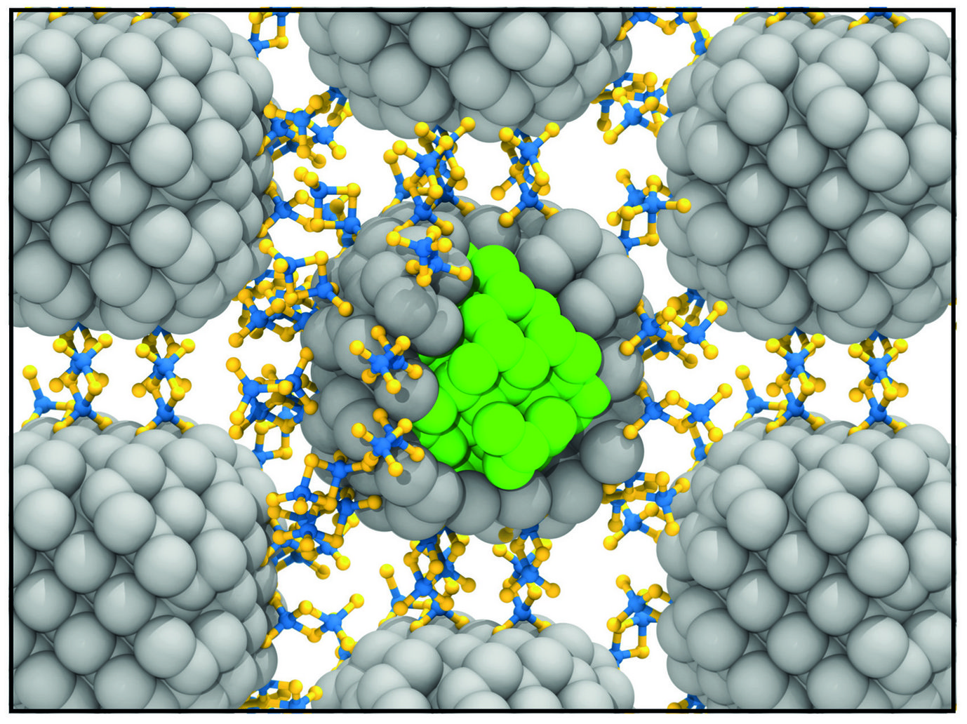
One possible route to create such nanostructured materials is to use colloidal nano-scale building blocks, e.g., nanocrystals, as “artificial atoms” and assemble them into quantum dot (QD) solids (Fig. 1). III-V semiconductor-based QDs, consisting of e.g., InP or InGaP nanocrystals, are among the most widely investigated materials systems due to their potentially superior optical properties and lower toxicity, compared to commercially available II-VI QD solids. Nevertheless, III-V systems still suffer from inferior colour purity due to broad emissivity and poor photoluminescence quantum yields. We recently demonstrated [1] that nanocrystal stoichiometry dispersion is a major source of trap states and largely responsible for the observed emission broadening in III-V QD solids. Whereas II-VI QD solids require only nanocrystal size control to achieve narrow emission, it is necessary to realize in addition nanocrystal stoichiometry control in the case of III-V QD solids.

Anomalously strong temperature-induced shifts of the electronic bandgaps are another important source of emission broadening. In order to reveal the origin of these anomalous shifts, we used so-called magic-sized nanoclusters as atomically precise model systems for nanocrystals with zero dispersion in both size and stoichiometry. Tantalizingly, approaches that are commonly employed to accurately predict temperature-dependent bandgaps in bulk materials have been known for more than a decade to yield qualitatively wrong results in the case of nanocrystals. We therefore developed a novel approach that allows us to accurately compute temperature-induced band gap shifts also for nanocrystals, using constrained ab initio molecular dynamics (AIMD) simulations on the excited state potential energy surface and atomistic thermodynamics, where the band gap is computed as the Gibbs free energy of exciton formation. The key innovation of our approach in contrast to existing methods is to take into account the fully anharmonic exciton-phonon coupling [2].
We revealed [2] that the experimentally observed anomalous colour shifts with temperature are caused by excitonic bond-softening: in nanocrystals, the excitons are distributed over only a small number of atoms due to the strong quantum confinement. In consequence, the occupation of antibonding states due to the presence of the excitons significantly weakens the interatomic bonds, leading to a pronounced exciton-induced red shift of the phonon density of states (PDOS). This shift is almost two orders of magnitudes larger than the corresponding one observed in bulk materials. The red-shifted PDOS in turn is responsible for the anomalous bandgap shift due to its impact on the Gibbs free energy of exciton formation. Our results underline the importance of explicitly considering exciton-electron-phonon coupling in nanostructures and suggest how to design systems with improved optical properties.
Moreover, the design of heterostructures at the nanoscale, such as multilayered structures consisting of CrN and AlN layers with a few nm thickness allows us to tune and tailor the mechanical properties for hard coating applications. In order to establish relations between the elastic properties, chemical composition and crystal structure, we investigated fast screening methods for fracture [3], but also applied novel scanning transmission electron microscopy-electron energy loss spectroscopy (STEM-EELS) methods to measure mechanical properties with nm high spatial resolution [4]. We analyzed AlN/CrN multilayers deposited epitaxially on MgO together with colleagues from Montanuniversität Leoben and TU Wien. The AlN layer thickness was increased from initially 1 nm to 10 nm, while the CrN layer thickness was kept constant at 4 nm (Fig. 2). Atomically resolved S/TEM reveals that AlN layers up to 4 nm grow in the metastable zincblende structure, while thicker AlN layers possess the room temperature stable wurtzite structure. The difference in crystal structure is also seen in the fine structure of the N-K edge in core loss EEL spectra as well as a shift in the plasmon peak positions for low loss EELS. The plasmon energy and the bulk modulus, which are related by an empirical relation established in literature were quantitatively extracted. Metastable cubic AlN, which allows for improved fracture toughness, was revealed to feature the highest bulk modulus values with 233±9 GPa in agreement with density functional theory (DFT) predictions [4].
![Fig 2: a) STEM-HAADF (high-angle annular dark field) image of CrN (bright) and AlN (dark) layers grown on MgO, with AlN layer thickness increasing from 1 nm to 10 nm from left to right. (b) Corresponding low loss EELS plasmon maps and (c) bulk modulus based on an empirical relation between plasmon energy and bulk modulus. Taken from [4].](/4690447/original-1643015834.webp?t=eyJ3aWR0aCI6MTY5NiwiZmlsZV9leHRlbnNpb24iOiJ3ZWJwIiwib2JqX2lkIjo0NjkwNDQ3fQ%3D%3D--ddb413e579c5aa2194a145462760299e1b15207a "Fig 2: a) STEM-HAADF (high-angle annular dark field) image of CrN (bright) and AlN (dark) layers grown on MgO, with AlN layer thickness increasing from 1 nm to 10 nm from left to right. (b) Corresponding low loss EELS plasmon maps and (c) bulk modulus based on an empirical relation between plasmon energy and bulk modulus. Taken from [4].")
![Fig 2: a) STEM-HAADF (high-angle annular dark field) image of CrN (bright) and AlN (dark) layers grown on MgO, with AlN layer thickness increasing from 1 nm to 10 nm from left to right. (b) Corresponding low loss EELS plasmon maps and (c) bulk modulus based on an empirical relation between plasmon energy and bulk modulus. Taken from [4].](/4690447/original-1643015834.jpg?t=eyJ3aWR0aCI6MTM3OCwib2JqX2lkIjo0NjkwNDQ3fQ%3D%3D--4d7578c292866f36581390eb41930cf7830692a4)
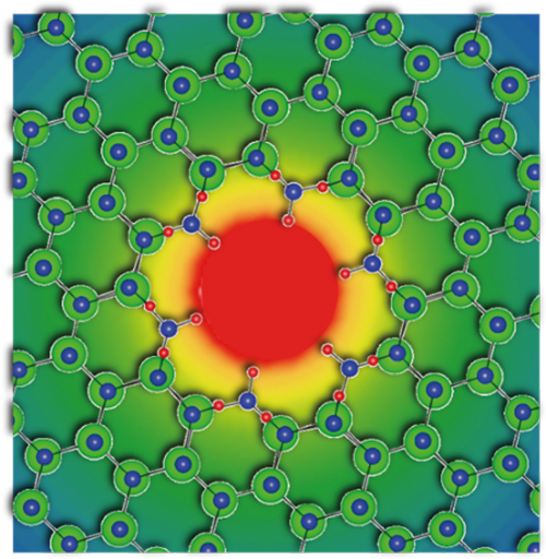
Epitaxial strain is the origin of the long standing and highly debated issue of threading dislocations in III-Nitride materials. Nevertheless, the topic has recently been reinvigorated due to the detrimental effect they have on power electronic devices. An intriguing feature of these defects is that experimental evidence suggests that screw dislocations are associated with open core structures, thus forming nanopipes (NPs). Although NPs exhibit large free surface areas which increase the energy, they can be energetically favourable if the surface energy is compensated by the core and strain energy of the material removed to create the NP.
In a recent study we combined DFT calculations with elasticity theory and we investigated the mechanisms governing the formation and the properties of nanopipes. Based on these calculations we constructed a screw dislocations’ phase diagram, which describes the energetically most favourable core structures as function of the species’ chemical potentials. A general trend that emerges from this diagram is that nanopipes are energetically favourable under typical MOCVD or MOVPE growth conditions. Under these conditions, the cation and anion dangling bonds at the open core inner surfaces are passivated by NHx molecules and H atoms, respectively (Fig. 3). This reduces considerably the surface energy and the formation of nanopipes with hexagonal cross section and equilibrium diameters ranging for ≈1 to ≈2 nm is energetically favourable. Nanopipes offer routes for efficient diffusion and the inner free surface sites for preferential incorporation of impurities. Indeed, our calculations indicate that both C and Mg dopants decorate the inner surface at concentrations (in at. %) at least one order of magnitude higher than in highly doped bulk semi-insulating layers [5].

The aforementioned examples from the fields of opto- and power electronics and hard coatings demonstrate that with our new methodological advances, both computational and experimental, it is now possible to reveal the complex interplay between the properties of materials at the nanoscale and their interaction with a complex growth environment. They also illustrate how our continued methodological developments guide novel applications design, and constitute an essential component in cutting-edge materials research and technology.
- Rusishvili, M.; Wippermann, S.; Talapin, D.; Galli, G.: Chem. Mater. 32 (2020) 9798.
- Muckel, F.; Lorenz, S.; Yang, J.; Nugraha, T. A.; Scalise, E.; Hyeon, T.; Wippermann, S.; Bacher, G.: Nature Comm. 11 (2020) 4127.
- Völker, B.; Du, C.; Fager, H.; Rueß, H.; Soler, R.; Kirchlechner, C.; Dehm, G.; Schneider, J. M.: Surf. Coat. Technol. 390 (2020) 125645.
- Zhang, Z.; Chen, Z.; Holec, D.; Liebscher, C. H.; Koutná, N.; Bartosik, M.; Zheng, Y.; Dehm, G.; Mayrhofer, P. H.: Acta Mater. 194 (2020) 343.
- Koller, C.; Lymperakis, L.; Pogany, D.; Pobegen, G.; Ostermaier, C.: J. Appl. Phys. 130 (2021) 185702.
- Yoo, S-H.; Lymperakis L.; Neugebauer J.: Phys. Rev. Mater. 5 (2021) 044605.


