Advanced electron microscopy techniques: in situ SEM/TEM and 4D-STEM
Electron microscopes offer unique capabilities to probe materials with extremely high spatial resolution. Recent advancements in in situ platforms and electron detectors have opened novel pathways to explore local properties and the dynamic behaviour of materials.
Within the scanning electron microscope (SEM), in situ mechanical measurements allow for investigation under variable testing conditions such as temperature and strain rate on a wide range of geometries fabricated using focused ion beam (FIB) milling. We develop novel microscale fracture testing geometries for in situ observation of crack growth. Further, a robust in situ SEM methodology has been recently designed for electrical measurements with high spatial resolution [1] and high sensitivity allowing for resistivity measurement of individual microstructural features such as grain boundary segments. Using the method, we successfully analyzed the resistivity-structure relations of grain boundaries and dislocations in Cu, thermoelectric materials [2] and metal oxides, while on-going research targets the effects of chemical segregation on local resistivity.
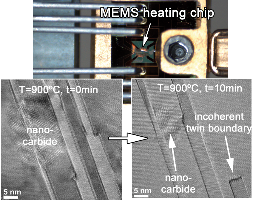
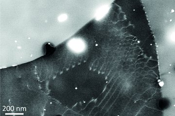
Aberration-corrected transmission electron microscopes (TEMs) enable the exploration of complex materials at atomic resolution. We develop novel sample preparation strategies, data acquisition schemes and algorithms to enable in situ heating observations down to atomic resolution. Our goal is to quantify the dynamic microstructure evolution of materials at elevated temperatures. We utilize micro-electro-mechanical systems (MEMS) based heating chips (Fig. 1) with ultra-high stability and temperature control. This system was used to explore novel precipitation pathways of nano-carbides in nano-twinned regions of interstitially alloyed high entropy alloys [3]. We further optimized sample geometries to explore their phase decomposition at 900 °C and atomic resolution (see Fig.1). The fast acquisition of high resolution data enables us to devise new algorithms to quantify the dissolution dynamics of the nano-carbides. Thermoelectric materials harvest energy from a temperature gradient, but the microstructures at the hot end are rarely characterized. Our recent study reveals that the dislocation networks designed to scatter phonons in PbTe can be stabilized at higher temperatures by pinning Cottrell atmospheres [4]. As another example, we observed Ostwald ripening in nanostructured oxides, which was beneficial to their photocatalytic activity [5].

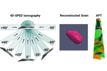
The advancement of fast electron detectors not only enables the dynamic observation of materials under in situ conditions with high time resolution, but also renders the development of novel imaging modalities possible. We advanced precession electron diffraction assisted 4D-STEM techniques, where a full electron diffraction pattern is captured at every beam position in a scanning TEM (STEM). These large-scale datasets provide rich crystallographic information of samples at nanometer resolution for extracting local grain and phase orientations in nanomaterials [6]. Ultimately, we strive to combine in situ probing with 4D-STEM to establish a complete quantitative picture of microstructure evolution.
- Bishara, H.; Ghidelli, M.; Dehm, G.: ACS Appl. Electron. Mater. 2 (7) (2020) 2049.
- Luo, T.; Serrano-Sánchez, F.; Bishara, H.; Zhang, S; Villoro, R.B.; Kuo, J.J.; Felser, C.; Scheu, C.; Snyder G.J.; Best, J.P.; Dehm, G.; Yu, Y.; Raabe, D.; Fu, C.; Gault, B.: Acta Mater. 217 (2021) 117147.
- Lu, W.; Liebscher, C.H.; Yan, F.; Fang, X.; Li, L.; Li, J.; Guo, W.; Dehm, G.; Raabe, D.; Li, Z.: Acta Mater. 185 (2020) 218.
- Abdellaoui, L.; Chen, Z.; Yu, Y.; Luo, T.; Hanus, R.; Schwarz, T.; Bueno Villoro, R.; Cojocaru-Miredin, O.; Snyder, G.J.; Raabe, D.; Pei, Y.; Scheu, C.; Zhang, S.: Adv. Funct. Mater. 31 (2021) 2101214.
- Zhang, S.; Diehl, L.; Wrede, S.; Lotsch, B.V.; Scheu, C.: Catalysts 10 (2020) 13.
- Jiwon, J.; Cautaerts, N.; Dehm, G.; Liebscher, C.: Microsc. Microanal. (2021) 1.
