Metal to charge density wave interfaces
Low dimensional electronic systems, featuring charge density waves and collective excitations, are highly interesting from a fundamental point of view. These systems support novel types of interfaces, such as phase boundaries between metals and charge density waves.
The Si(111)-(4x1)/(8x2)In nanowire array is a prototypical model surface for a temperature-induced metal to charge density wave (CDW) transition. CDW formation is driven by a triple-band Peierls transition in conjunction with three soft phonon modes. As demonstrated in our "ultrafast dynamics" project the transition is first order. Here, we show that both phases can coexist and form a novel type of electronic interface: a metal-CDW interface.

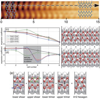
Interestingly, these interfaces can form as extended structures with the electronic phase changing gradually over a length of more than 10 lattice constants a0 along the wire direction, see figure. At point defects however, the electronic structure changes abruptly from insulating to metallic within a single a0.
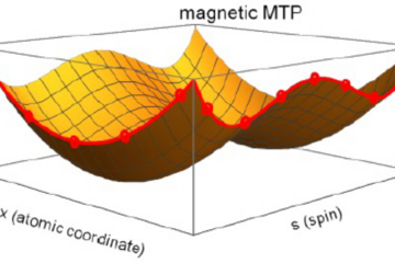
We showed that the gradual interfaces are dynamic in nature. Both the insulating and the metallic phase are local minima on the potential energy surface with equal depth at the transition temperature, separated by an energy barrier. Thermal excitation of the soft phonon modes that drive the phase transition lead to dynamical fluctuations between the two phases, giving rise to the extended interface observed by scanning tunneling microscopy (STM) measurements. See our soliton project for further information on the phonons.
In conjunction with STM data, we reveal that only a particular defect leads to abrupt metal-CDW interfaces: an additional In adatom adsorbed on top of the wire. This defect effectively pins the soft phonons responsible for the dynamic fluctuations, collapsing the wire into a specific state at either side of the defect. This model is corroborated by ab initio molecular dynamics simulations, where the trajectories are expanded in terms of the phonon eigenvectors as a basis set.
STM simulations for the averaged structures compare extremely well to the STM measurements. The resulting structures are an optimal starting point to now explore the electronic properties of metal-CDW interfaces. This work is strongly connected to our soliton project, where the same structural motifs and defects play a prominent role.
