Combinatorial approach to tailor electrical and mechanical properties of alloyed thin film structures
Copper is widely used in micro- and nanoelectronics devices as interconnects and conductive layers due to good electric and mechanical properties. But especially the mechanical properties degrade significantly at elevated temperatures during operating conditions due to segregation of contamination elements to the grain boundaries where they cause grain boundary embrittlement and promote mechanical failure, limiting the lifetime of devices.
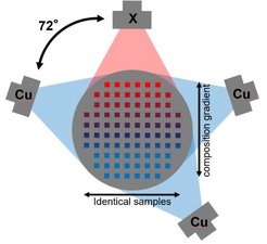
The focus of this study is the synthesis of Cu alloys by combinatorial thin film deposition techniques to investigate the strengthening and structural effects of different second elements through grain boundary doping.
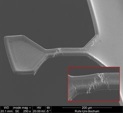
As a second focus, photolithographic methods for the fabrication of microscale tensile samples for the investigation of mechanical properties are investigated. With such a photolithographic process, it is possible to rapidly fabricate significant numbers of samples for mechanical testing in a short time, possibly providing a significant time saving over traditional sample fabrication such as ion beam milling.