Electron channeling contrast imaging - ECCI
ECCI is an imaging technique in scanning electron microscopy based on electron channelling applying a backscatter electron detector. It is used for direct observation of lattice defects, for example dislocations or stacking faults, close to the surface of bulk samples.

Understanding ECCI is done best by looking into the physics of interaction of an electron beam with a crystal: When high energy primary beam electrons of a scanning electron microscope enter into a crystalline sample they form a standing electron-density wave inside the lattice which is coherent with the crystal lattice, the so-called primary wave field. Depending on the direction of the primary electron beam with respect to the lattice the maxima of the electron density waves may change from a position at the atomic nuclei to one in between them. In the first case strong backscattering of electrons out of the primary wave field occurs, while in the latter case only few electrons are backscattered. As a consequence, the backscatter signal carries information about the crystal lattice and its orientation relative to the primary beam. Minimum backscattering occurs when the primary beam almost exactly fullfills the Bragg angle with one of the lattice planes. The electrons then travel deep into the crystal without intense interaction with it. This case is called electron channelling.
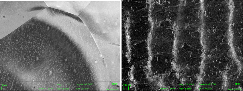
If a defect, e.g. a dislocation or a stacking fault is present in the crystal then the coherency of the channelling primary electron wave field with the lattice is disturbed and strong backscattering occurs at the position of the defect. As a result, the defect is visible as a bright feature on an otherwise dark background when the sample is observed with a backscatter electron detector.
ECCI shows very comparable contrast features to dark-field TEM with the advantage that the images are obtained on bulk samples rather than on thin foils. In contrast, resolution and contrast are less good than in TEM.
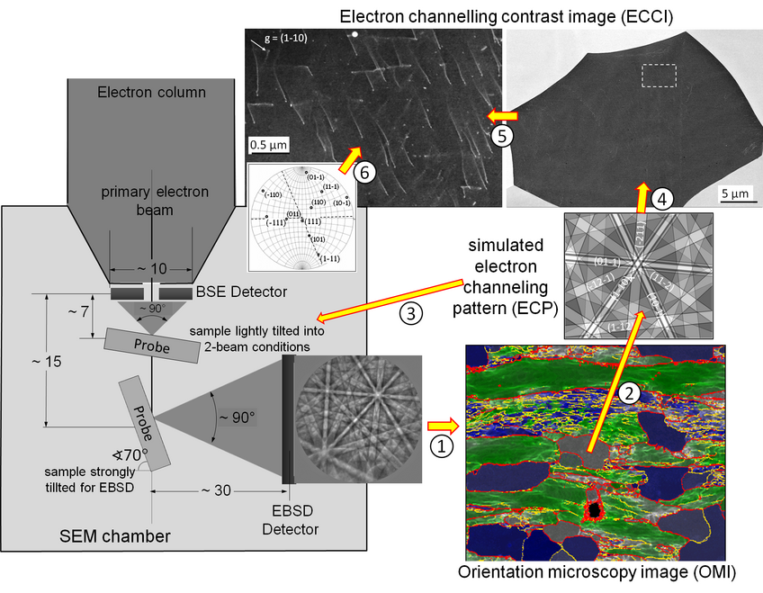
When conventionally applying the ECCI technique for defect observation in a polycrystalline sample, it is not known which lattice plane leads to the observed defect contrast and whether the exact channeling conditions are excited. This can be corrected for by measuring the crystal orientation with EBSD or with ECP (electron channeling pattern). When ECP is available (which is rarely the case on modern microscopes) then the channeling contrast can be directly selected by tilting the sample until a channeling (or Kikuchi) line runs through the centre of the pattern. Subsequently, the microscope is run in scanning mode and the desired channelling contrast is observed. When the orientation is measured by EBSD, a software is required to emulate the theoretically obtained EC pattern based on the measured orientation. This software also emulates the sample tilt required to obtain good channelling conditions. The software-determined tilt conditions are subsequently set to the microscope stage and channelling contrast is observed.
We call the control of the channelling conditions via ECP or EBSD technique as "Electron channeling contrast imaging under controlled diffraction conditions", short cECCI. The figure below shows a schematics of this technique: (1) determination of a crystal orientation via EBSD. (2) Simulation of an ECP for the position of interest using the computer program TOCA. This program is also used to determine the tilt angles required for two-beam conditions. (3) Positioning of the sample as determined in step (2). (4) and (5) Observation of the channelling contrast. (6) Crystallographic interpretation of the channelling contrast using, for example, TOCA.

