Challenges of ECCI on light metals
Electron channelling contrast imaging (ECCI) is a powerful technique for observation of extended crystal lattice defects (e.g. dislocations, stacking faults) with almost transmission electron microscopy (TEM) like appearance but on bulk samples in the scanning electron microscope (SEM).
ECCI has been proven to give good results on materials that have an average atomic number larger than approx. 20 (calcium). Titanium, steels, Ni-base alloys, tungsten, pyrite (FeS2), CdTe, and many other metals and compounds give very good channelling contrast. In contrast, for the lighter materials, e.g. silicon, aluminium, magnesium and many minerals, e.g. quartz, the contrast is significantly worse and achieving proper channelling is challenging. The reasons for this are manifold: the most important is the lower electron scattering power of the lighter elements, but lower crystal symmetry and preparation artefacts, among others, also play a role.
Due to the lower scattering power the primary electrons penetrate deeper into the material. As a result the electron wave “senses“ the atom channels of the crystal to a larger depth below the surface, which means that the beam may have a higher probability to encounter atom columns, bent due to the presence of elastic strains. As a consequence, an original channelling situation (allowing visualization of lattices defects) may turn into a backscattering one (which veils lattice defects). This happens particularly on ductile metal, and may strongly reduce the channelling contrast and visibility of defects. Even slightly deformed light metals may, therefore, not show any useful channelling contrast.
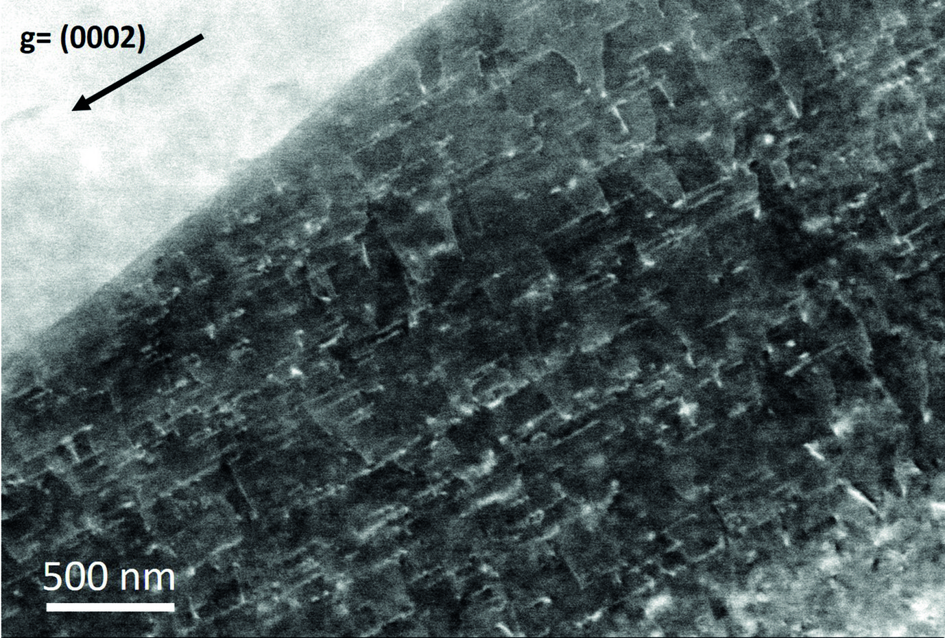
The most efficient way to handle the lower scattering power is to reduce the acceleration voltage. This increases contrast and allows in many cases to observe good channelling contrast on light metals. Fig. 1 displays an example of a small angle grain boundary in a 7075 aluminium alloy, solution annealed and slightly aged, imaged at 20 kV (instead of the usual 30 kV). An electro-polishing procedure at low temperatures (-30 °C) excluding water allowed proper ECCI preparation of the material.

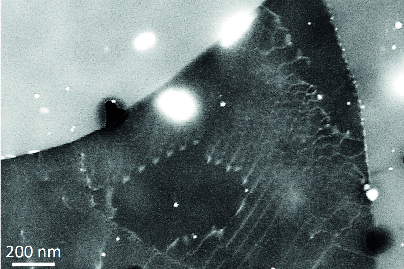
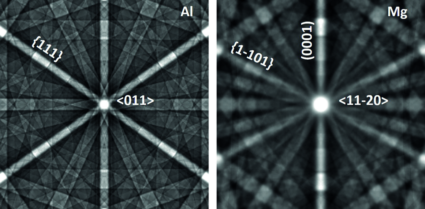
The case of magnesium is even more challenging than that of aluminium. First, Mg creates an even thicker oxide film than Al-Zn alloys which prevents from “seeing through it” with low energy electrons. Final preparation needs to be done by extended ion polishing. A second, and equally important reason is the hexagonal closed packed (hcp) crystal structure. Compared to the face centred cubic (fcc) structure, the diffraction intensities are much reduced and less homogeneously distributed over reciprocal space. In fact, the strongest reflector in the hcp structure is the (0001) plane of which only one exists. In the cubic structure the {111} planes (4) and the {011} planes (6) all allow good imaging. This fact is displayed in fig. 2, showing simulated electron channelling patterns for Al and Mg. Nevertheless, if preparation is optimum and the strongest reflectors are used for imaging, dislocation structures may be visualized very well also in Mg alloys. An example is shown in fig. 3 displaying the <c+a>-type dislocations that form inside of extension twins. And also here the advantages of ECCI over TEM, namely observation of large bulk samples and performance of in situ experiments, may be highly valuable.
 and hcp Mg (Z=12). Al shows much stronger, sharper and more homogeneously distributed reflectors.")
 makes dislocations visible.")