Correlative Use of Atom Probe Tomography and Electron Microscopy
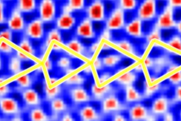
Many fundamental phenomena in materials science such as the segregation to defects, elemental partitioning, nucleation, deformation-driven phase decomposition, or spinodal decomposition need to be understood at the atomic scale, requiring mapping of local chemical composition and crystallography.
M. Herbig*, O. Cojocaru-Mirédin*,1, W. Guo*,2, A. Stoffers*, T. Schwarz*, M. Kuzmina*, Y. Toji*,3, M. Yao*, E. Welsch*, M. Köhler*, S. Zaefferer*, P.-P. Choi*,4, D. Raabe*
*Department of Circular Metallurgy and Alloy Design
1now at: Institute of Physics (IA), Rhein-Westfälische Technische Hochschule Aachen (RWTH)
2now at: Center for Nanophase Materials Sciences, Oak Ridge National Laboratory, Oak Ridge, USA
3now at: Steel Products Research Department, JFE Steel Corporation, Kawasaki, Japan
4now at: Korea Advanced Institute of Science and Technology (KAIST), Daejeon, South Korea
This requires the development of suited characterization techniques. Atom probe tomography (APT) with its capability of detecting 3D elemental distributions with near atomic spatial resolution and a sensitivity in the range of 10 parts per million, which is independent of the atomic number [1] is currently the best high resolution tool for quantifying local chemical inhomogeneity. However, its spatial resolution is material dependent and often not accurate enough to capture crystallographic aspects such as defect type, grain orientations or phase crystallography. In these cases transmission electron microscopy (TEM) is better suited. But this technique lacks accuracy in quantifying chemical composition, especially in the case of light elements, high dilution and non-planar features. Thus, TEM and APT have complementary strengths and their correlated application to the same specimen provides joint chemical and structural insights to some of the main pending fundamental scientific questions in materials science.
![Figure 1: The correlative use of TEM (a) and APT (b) enables mapping both, structural and chemical information of the same sample at the nanometer scale [3].](/3750260/original-1518446901.jpg?t=eyJ3aWR0aCI6OTY2LCJvYmpfaWQiOjM3NTAyNjB9--ab8487dfd3c4971eebcf66afdec0a255a2c2f59b)
Figure 1: The correlative use of TEM (a) and APT (b) enables mapping both, structural and chemical information of the same sample at the nanometer scale [3].
Over the past four years an experimental setup and corresponding know-how has been developed at MPIE rendering correlative TEM /APT experiments feasible and robust [2]. This work led so far to several high impact publications: for the first time nanobeam diffraction (NBD) orientation mapping was used on atom probe tips, thereby enabling the high throughput characterization of grain boundary segregation [3] (Figure 1) as well as the crystallographic identification of phases [4]. Bright-Field STEM imaging enabled to prove the existence of linear complexions [5] and to map atomistic details associated with shear-induced mixing [6]. The spectrum of TEM/APT techniques is currently expanded to the correlative use of Dark-Field TEM and APT. Owing to the experimental efforts involved in correlative TEM/APT all scientific cases that do not require the spatial resolution of a TEM should be investigated by scanning electron microscopy (SEM). Therefore, SEM-based approaches to gather crystallographic information on atom probe samples have been developed [7,8]. Future plans involve the use of Electron Channeling Contrast Imaging under controlled geometric conditions (cECCI) [9] on atom probe samples that has the potential to speed up the site-specific sample preparation of crystal defects and their analysis. Intense collaborations with the department “structure and nanomechanics” are planned to combine latest high-resolution TEM instruments with a new atom probe with up to 80% detector efficiency.
References
[1] T. F. Kelly and D. J. Larson, Annu Rev Mater Res 42, 1 (2012).
[2] M. Herbig, P. Choi, and D. Raabe, Ultramicroscopy 153, 32 (2015).
[3] M. Herbig, D. Raabe, Y. J. Li et al., Phys Rev Lett 112 (2014).
[4] Y. Toji, H. Matsuda, M. Herbig et al., Acta Materialia 65, 215 (2014).
[5] M. Kuzmina, M. Herbig, D. Ponge et al., Science 349, 1080 (2015).
[6] W. Guo, E. A. Jagle, P. P. Choi et al., Phys Rev Lett 113 (2014).
[7] M. Herbig, M. Kuzmina, C. Haase et al., Acta Materialia 83, 37 (2015).
[8] A. Stoffers, O. Cojocaru-Mirédin, W. Seifert et al., Progress in Photovoltaics (2015).
[9] S. Zaefferer and N. N. Elhami, Acta Materialia 75, 20 (2014).
![Figure 1: The correlative use of TEM (a) and APT (b) enables mapping both, structural and chemical information of the same sample at the nanometer scale [3]. Figure 1: The correlative use of TEM (a) and APT (b) enables mapping both, structural and chemical information of the same sample at the nanometer scale [3].](/3750260/original-1518446901.jpg?t=eyJ3aWR0aCI6MzQxLCJmaWxlX2V4dGVuc2lvbiI6ImpwZyIsIm9ial9pZCI6Mzc1MDI2MH0%3D--1d13accdfffb07b9bfc711f24b3f756441732e00)
