Green energy: How to increase the efficiency of solar cells
Max Planck scientists publish their findings in the journals Nature Communications and Nano Energy
How to increase the efficiency of solar cells and thus pave the way for a higher usage of green energy in industry? Dr. Torsten Schwarz, senior researcher in the group “Nanoanalytics and Interfaces” at the Max-Planck-Institut für Eisenforschung, analysed how surface treatments of chalcogenide semiconductors influence their defect concentrations and thus their performance and which adjustments during the manufacturing of solar cells are needed to achieve a better performance. Together with colleagues mainly from the University of Luxembourg, he published their findings in the journals Nature Communications and Nano Energy.

“Understanding the nature of defects, their concentration and mobility during growth is decisive for the design of many technologies. We already know that we can influence the properties of semiconductors used in photovoltaic applications by subtle changes of their growth conditions during manufacturing. At the same time, changing the growth conditions implies a varying chemical potential, which may lead to instable interfaces favouring detrimental chemical reactions. In the case of the chalcogenide semiconductor CuInSe2 (CISe), which we use, such detrimental reactions can occur at the surface.”, explains Schwarz. The growth of CIS thin-films typically passes the phase boundary from Cu-poor to Cu-rich and back to Cu-poor in order to combine the superior microstructure of Cu-rich films and the superior electrical properties of Cu-poor films to achieve the highest solar cell efficiency. However, although Cu-rich films show a better fingerprint of their optical properties, it was till now unknown why these films show a worse performance than their Cu-poor counterparts. Another unsolved question concerns the effect of defect concentrations on the device’s performance. These defects are caused by surface treatments during the solar cell’s manufacturing, especially while the cell is subjected to ambient air, chemical etchants and post-deposition treatments, before being protected by a buffer layer. “Our work reveals that the exposure of the CISe surface to ambient air causes even at room temperature the spontaneous formation of In2O3 and Cu2Se secondary phases. This reaction takes place much faster in the Cu-rich samples, since it is presumably catalyzed by the very mobile and excess Cu atoms.”, states Schwarz. A key to obtain this result was the use of atom probe tomography to prove that domains of only a few nanometers in size with an excess of Cu actually exist. Cyanide etching is needed to remove the detrimental Cu2Se, which would otherwise lead to a failure of the final device. However, this necessary etching step does not only remove Cu2Se on the surface but also Cu and Se atoms up to several tens of nanometer below the surface. The Cu and Se depletion leads to the formation of Cu-Se divacancies defects. These defects cause a significant loss in open-circuit voltage. They also exist in Cu-poor CISe films, but with a much smaller concentration, and can be removed completely by depositing of a buffer layer. “Specific chemical treatments with group VI elements, such as O, S, and Se can occupy the anion vacancies and thus passivate the divacancies. If we pay a special attention to those post-treatments, we can increase the performance of solar cells.”, says Schwarz.
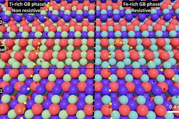
In another paper Schwarz and his colleagues from the MPIE and the University of Luxembourg investigated CuInS2 (CIS) thin-films, which are used in tandem solar cells. The question here was, which other adjustments can be made to increase the efficiency if the defects caused by the post-treatment can be overcome. Therefore, the team of scientists has investigated the microstructure of these films, especially the composition of defects such as grain boundaries. “We used correlated atom probe tomography and electron backscatter diffraction to investigate the relationship between the chemistry and the structure of these defects. In our work, we show that the grain boundaries in Cu-rich and Cu-poor films have very contrary compositions. While so-called random grain boundaries in the Cu-poor film show Cu depletion and In enrichment, these grain boundaries in the Cu-rich film show Cu enrichment and In depletion. We were also able to confirm this phenomenon for a special type of grain boundaries, the so-called ∑9 twin boundaries. But even more interesting is that, although both films had been grown on a glass substrate and, therefore, the same impurities were suspected at random grain boundaries, we detected only in the Cu-poor sample Na and K impurities. On the contrary, in the Cu-rich films we found unexpectedly C at random grain boundaries in addition to Na. Moreover, ∑3 twin boundaries, showed no chemical fluctuations at all in both films.”, explains Schwarz.
The scientists are now heading to understand the origin and the effects of post-treatment and the passivation of grain boundaries in Cu-rich CIS films on the overall performance of solar cells.
Nature Communications 11 (2020) 3634
Nano Energy 76 (2020) 105081
Text: Torsten Schwarz, Yasmin Ahmed Salem


