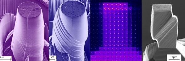
Influence of microstructural constraints on slip transfer in nanotwinned Ag
Nanotwinned Ag thin films were deposited in house by e-beam evaporation in a BESTEC PVD cluster. The twin spacing was varied from 20nm to 1μm with suitable thermal treatment. In order to study the dislocation-CTB interactions, micropillar compression tests were carried out on pillars with varying twin spacing. Perfect slip transfer was observed down to the scale of nanotwins despite increase in yield strength at smaller twin spacings. The study addresses size scaling due to weak constraints for dislocation motion and underlying deformation mechanisms. Further microscale behavior is compared with the bulk deformation behavior of thin films studied using wafer curvature and nanoindentation measurements.
See also: "Dislocation-coherent twin boundary interactions in FCC metals: Size Scaling"

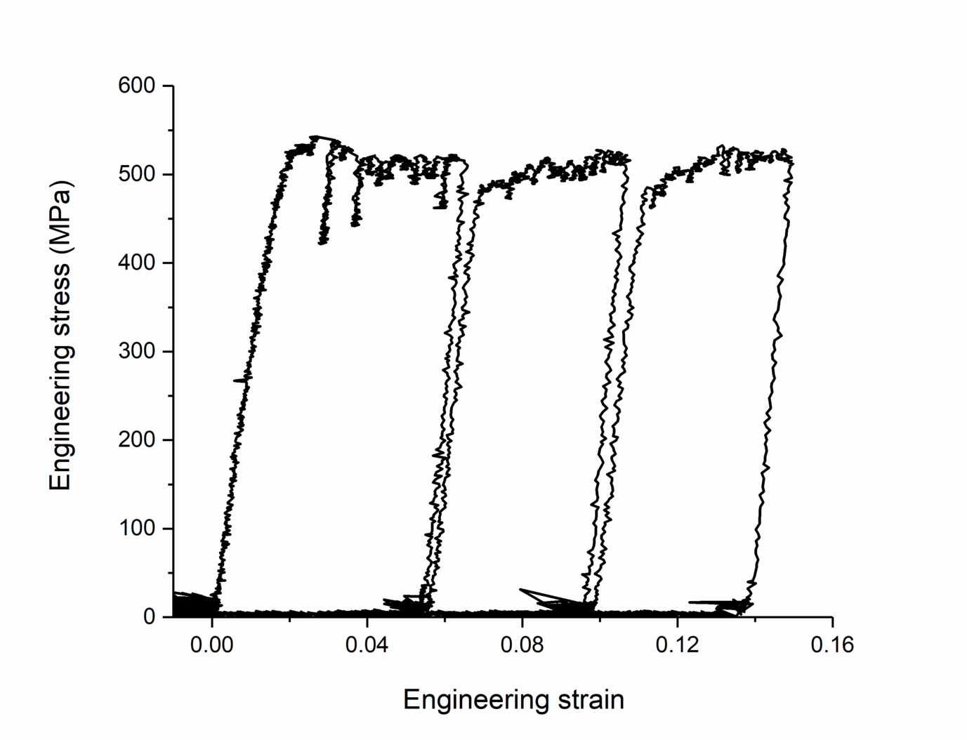
Figure 1: Typical engineering stress – engineering strain curve for nanotwinned Ag with a twin spacing of ~ 20 nm

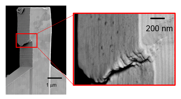
Figure 2: Slip steps on the surface of a deformed nanotwinned Ag micropillar.

