CdTe solar cell material
Cadmium telluride (CdTe) belongs to the II-VI semiconductors family, together with other notable compounds such as cadmium sulfide (CdS), zinc oxide (ZnO) or zinc selenide (ZnSe). Its direct bandgap of 1.5 eV at room temperature matches perfectly the requirement for highly efficient sunlight energy conversion, allowing a theoretically predicted maximum efficiency of around 32 %.
Text by Guillaume Stechmann (MPIE)
Besides its almost ideal bandgap, its absorption coefficient, i.e. its propensity to convert photon energy into mobile charge carriers, is remarkably high, thus reducing the amount of material needed in the design of absorber layers and as such, production costs. As a comparison, typical commercial silicon-based solar cells require an absorber thickness of around 200 mm whereas their CdTe equivalents are less than 5 mm thick. [1-2]
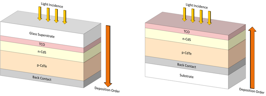
Two typical configurations, based on the CdTe/CdS p-n junction can be used in the design of such solar cells. On the one hand, the most common “superstrate configuration” which follows the stacking sequence glass superstrate / transparent conductive oxide / CdS / CdTe / back contact, have demonstrated the best efficiencies thanks to easier doping and a better control of the CdTe / back contact interface. On the other hand, the more recently-developed “substrate configuration”, whose stacking sequence is reversed and follows the order substrate / back contact / CdTe / CdS / transparent conductive oxide, enables deposition on flexible and metallic substrates for new types of applications and process cost reduction. [1-3]

Right: Substrate configuration
As of 2015, CdTe-based solar cells are one of the cheapest available on the market and contribute to the production of around 2 GW of electricity per year worldwide. This is about the total annual electricity consumption of Iceland or one month in Australia. Moreover, best laboratory cells can reach efficiencies up to 21 % whereas large-scale modules overcame the 17 % barrier. [4-7]
In contrast to the general believe, cadmium telluride solar cells have been reported to be the most “eco-friendly” commercial photovoltaic system, beating silicon and CIGS technologies in term of energy payback time and carbon footprint. Furthermore, concerns regarding the presence of cadmium have been discarded by numerous studies, accounting for the very high melting point and stability of CdTe combined with modern encapsulation techniques. [7-8]
The main challenge regarding efficiency improvements of such materials remains the relatively low open circuit voltage of CdTe/CdS cells. Best obtainable voltages are indeed in the range of 850-900 mV whereas values in the order of 1.2 V could be expected in respect to the absorber layer band gap. This limitation is linked to the photo generated carriers lifetime which is, in return, affected by the layer microstructure. Therefore, optimizing CdTe thin films microstructure would result in an increased efficiency.
[1] Durose, K. et al., Journal of Crystal Growth, 197, 733-742, 1999
[2] Bonnet, D. and Meyers, P., Journal of Materials Research, 13, 2740-2753, 1998
[3] Gretener, C. et al., Progress in Photovoltaics: Research and Applications, 21, 1580-1586, 2013
[4] The CIA World Factbook, Electricity Consumption, https://www.cia.gov/
[5] Fraunhofer Institute for Solar Energy System ISE, Photovoltaics Report, 2014
[6] First Solar, First Solar Builds the Highest Efficiency Thin Film PV Cell on Record, http://investor.firstsolar.com/
[7] de Wild-Scholten M. J., Solar Energy Materials and Solar Cells, 119, 296-305, 2013
[8] Fthenakis, V. M., Renewable and Sustainable Energy Reviews, 8, 303-334, 2004
