One of the controversial issues in the field of III-Nitrides is the effect dislocations have on the optoelectronic properties of the devices.
For edge dislocations, we have shown in an earlier study that even in the case of fully coordinated cores the huge strain field around the dislocation line introduces deep states in the bandgap. The strain field of screw type dislocations is characterized by non-zero shear components and has been proposed to result in hole localization.
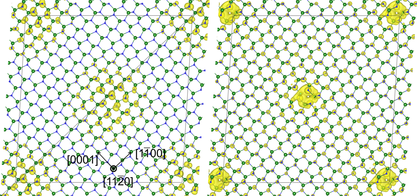
In this project we developed an ab-initio based quasi-static approach which combined density functional theory calculations with elasticity theory and we investigate the electronic properties of a-type screw dislocations in GaN.
In contrast to previous models where only a localization of the holes was considered, our calculations show a localization of both electrons and holes in the dislocation strain field. This field causes a mixing of the s-type state at the conduction band minimum (CBM) with the next highest state that has p character and is thus susceptible to the shear strain induced by the dislocation.
Surface energies, referenced with respect to the SiGaN3 terminated surface, as function of the number of GaN overlayers grown above the SiGaN3 layer. The upper left and right insets represent the atomic configurations without and with two GaN overlayers ontop the SiGaN3 mask, respectively. In the case of 2 GaN overlayers the charge transfer and the build in electrical dipole moment are indicated. The bottom right inset represents a top view of the SiGaN3 layer. The dashed frame indicates the √3×√3 R30o reconstruction. Green, blue, red, and white balls indicate Ga, N, Si atoms and Ga vacancies, respectively.
Surface energies, referenced with respect to the SiGaN3 terminated surface, as function of the number of GaN overlayers grown above the SiGaN3 layer. The upper left and right insets represent the atomic configurations without and with two GaN overlayers ontop the SiGaN3 mask, respectively. In the case of 2 GaN overlayers the charge transfer and the build in electrical dipole moment are indicated. The bottom right inset represents a top view of the SiGaN3 layer. The dashed frame indicates the √3×√3 R30o reconstruction. Green, blue, red, and white balls indicate Ga, N, Si atoms and Ga vacancies, respectively.