Understanding the effect of growth conditions on secondary phase formation, microstructure and optoelectronic properties of CZTSe thin-film solar cells
Thin-film solar cells based on the kesterite structured compound semiconductor Cu2ZnSn(S,Se)4 (CZTSSe) comprise inexpensive, earth-abundant, and non-toxic elements while maintaining favorable, optical, electrical properties (such as high absorption coefficient).

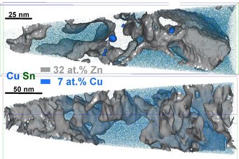
APT 3D map showing the secondary phase formation in CZTS kesterite solar cells.
Thin-film solar cells based on the kesterite structured compound semiconductor Cu2ZnSn(S,Se)4 (CZTSSe) comprise inexpensive, earth-abundant, and non-toxic elements while maintaining favorable, optical, electrical properties (such as high absorption coefficient). Currently, a major factor impeding the fabrication of high-performance CZTSSe solar cells is the narrow homogeneity range of CZTSSe, hence the formation of secondary phases like Zn(S,Se), Cu-(S,Se) and Cu-Sn-(S,Se) is likely. In order to improve the efficiency we characterize the absorber layer in detail.
STEM-EDX is used to identify and localize secondary phases, whereas APT is employed to investigate phase and grain boundaries as well as segregation of impurities at the atomic scale [1-2]. APT results are used for further first-principle calculations. Furthermore, EBSD and TEM are utilized to investigate the microstructure of the absorber layer and are correlated with the optoelectronic properties obtained by Cathodoluminescence measurements. The aim is to gain a better understanding of secondary phases, GBs and impurities and their effect on device performance. The work is done in collaboration with the University of Luxembourg and Lyon.
