Precision Epitaxy in Nanocrystalline Thin Films: Defect‑Tailored Platforms for Electrocatalysis
- Date: Jul 23, 2025
- Time: 02:00 PM - 03:00 PM (Local Time Germany)
- Speaker: Dr. Myoung Hwan Oh
- Department of Energy Engineering, Korea Institute of Energy Technology (KENTECH)
- Location: Max Planck Institute for Sustainable Materials
- Room: Large Conference Room No. 203
- Host: on invitation of Prof. Christina Scheu and Prof. Gerhard Dehm

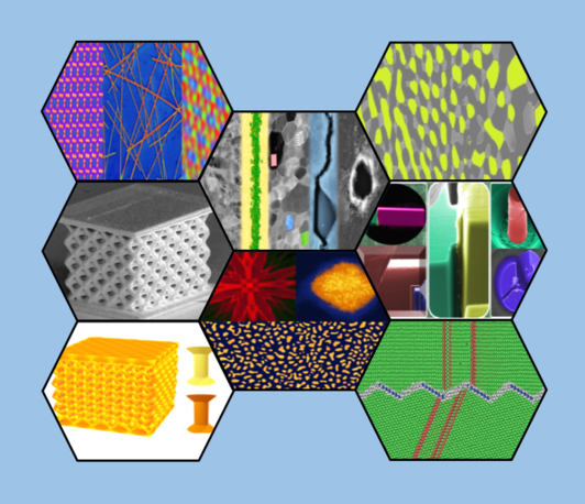
Topological defects—dislocations, grain boundaries, and related features—play an essential role in determining the properties of crystalline materials. When crystallite or functional domain sizes shrink to the nanometer scale, these defects become dominant. To date, however, neither bottom‑up nor top‑down synthesis has provided a reliable means of controlling them. Here, we demonstrate delicate control over shell epitaxy on nanocrystals within thin films, producing three‑dimensionally organized nanocrystallites with uniform grain boundaries and associated defects. In these structures, the resulting 3D‑patterned strain field can be mapped with atomic precision and tuned to introduce targeted dislocations or disclinations. Using multiscale crystallography and spectroscopy, we show that the uniformity and discreteness of these defects provide a clear correlation between local structure and collective electrochemical performance—specifically, catalytic activity in oxygen evolution and reduction reactions. Finally, we outline how this nanocrystallite‑engineering approach is guiding the design of next‑generation functional materials for energy nanotechnology