Scientific Events

Location: Max Planck Institute for Sustaianble Materials

Precision Epitaxy in Nanocrystalline Thin Films: Defect‑Tailored Platforms for Electrocatalysis

Topological defects—dislocations, grain boundaries, and related features—play an essential role in determining the properties of crystalline materials. When crystallite or functional domain sizes shrink to the nanometer scale, these defects become dominant. To date, however, neither bottom‑up nor top‑down synthesis has provided a reliable means of controlling them. Here, we demonstrate delicate control over shell epitaxy on nanocrystals within thin films, producing three‑dimensionally organized nanocrystallites with uniform grain boundaries and associated defects. In these structures, the resulting 3D‑patterned strain field can be mapped with atomic precision and tuned to introduce targeted dislocations or disclinations. Using multiscale crystallography and spectroscopy, we show that the uniformity and discreteness of these defects provide a clear correlation between local structure and collective electrochemical performance—specifically, catalytic activity in oxygen evolution and reduction reactions. Finally, we outline how this nanocrystallite‑engineering approach is guiding the design of next‑generation functional materials for energy nanotechnology [more]

Big data microscopy: Machine learning-driven statistical characterization of shape evolution in nanoparticle growth

Understanding the geometry of nanomaterials at the atomic scale provides critical insights into local structural heterogeneities and their impact on functional properties. Since shapes vary from particle to particle, detailed analysis at the single-particle level is essential. In this talk, I will present a high-throughput pipeline that integrates deep learning-based segmentation with quantitative shape analysis of individual nanoparticles from high-resolution transmission electron microscopy (HRTEM) images. First, I will describe the application of convolutional neural networks (CNNs) to segment 727 HRTEM micrographs of cubic Co3O4 nanoparticles, enabling the extraction of shape descriptors from 441,067 particles. This automated workflow allows for population-wide statistical characterization, bridging local structural detail with large-scale analysis. Second, I will present a size-resolved shape analysis at subnanometer precision, highlighting a critical threshold, “onset radius”, that marks transitions in particle shape, such as surface faceting and a shift from thermodynamic to kinetic growth regimes. This bottom-up approach illustrates how machine learning and data-driven analysis can reveal previously unquantified trends, offering a generalizable framework for high-throughput materials characterization. [more]
Recent studies have shown that the passage of an electric current pulse may both propagate [1,2] and close a crack and heal a metallic material [3]. Specifically, experiments on thin Al foils containing edge cracks have proved that the self-induced electromagnetic forces, spontaneously generated upon passage of an electric current across a crack in a sample, alone could cause crack propagation without melting of the crack tip [1]. The critical current density required for crack propagation reduces in the presence of an external magnetic field [4] as well as mechanical load [5]. On the other hand, if an electric current pulse of large pulse width is passed through an electrically and thermally resistive material, such as stainless steel, containing a short crack, the crack may completely close, and the material can heal through the solid-state diffusion bonding process [3]. Here, we discuss the reasons behind crack propagation upon application of electric current and then explore the mechanics as well as microstructural attributes responsible for a transition from flaw propagation to flaw healing upon passage of an electric current pulse. Furthermore, the recovery of the mechanical properties of the material upon electric current-induced healing will also be discussed. [more]
Defects and Grain boundaries have a remarkable effect on the thermal and electrical transport properties of polycrystalline materials but are often ignored by prevailing physical theories. The concentration of point defects can be altered with phase boundary mapping considering the defect thermodynamics. Thus, the properties can be engineered with careful processing control. Grain boundaries and interfaces can adversely alter the thermal and electrical properties of Power Electronics, Solar Cells, Batteries, Thermoelectrics and permanent magnets such as interfacial electrical and thermal resistance (Kapitza resistance). Interfacial thermal resistance limits the performance of power electronics because of overheating. New scanning thermal reflectance techniques can image the thermal resistance of interfaces and boundaries directly. The Thermal conductivity suppression at grain boundaries can even be imaged showing that different grain boundaries can have very different thermal resistances with high energy grain boundaries having more resistance and low energy boundaries having lower thermal resistance. Interfaces and grain boundaries are 2-dimensional thermodynamic phases (complexions) that have distinct energy, composition and properties that can be rigorously described using the Gibbs excess formalism. The common thermodynamic quantities of temperature and chemical potential connects the complexions to the 3-D phases allowing a phase boundary mapping of grain boundary and interface properties similar to that for point defects. [more]

Fracture at the Two-Dimensional Limit

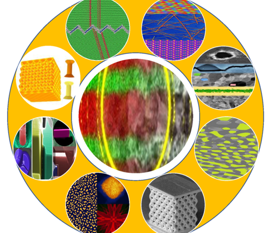
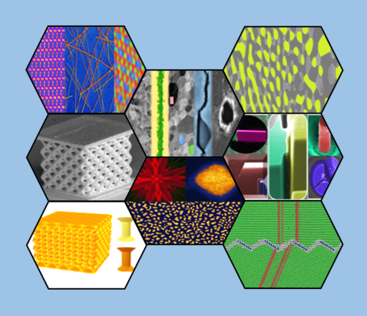
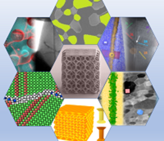
Two-dimensional (2D) materials, such as Graphene, hBN, and MoS2, are promising candidates in a number of advanced functional and structural applications owing to their exceptional electrical, thermal, and mechanical properties. Understanding the mechanical properties of 2D materials is critically important for their reliable integration into future electronic, composite, and energy storage applications. In this talk, we will report our efforts to study the fracture behaviors of 2D materials. Our combined experiment and modelling efforts verify the applicability of the classic Griffith theory of brittle fracture to graphene [1]. Strategies on how to improve the fracture resistance in graphene, including a nanocomposite approach, and the implications of the effects of defects on mechanical properties of other 2D atomic layers will be discussed [2, 3]. More interestingly, stable crack propagation in monolayer 2D h-BN is observed and the corresponding crack resistance curve is obtained for the first time in 2D crystals [4]. Inspired by the asymmetric lattice structure of h-BN, an intrinsic toughening mechanism without loss of high strength is validated based on theoretical efforts, enabling stable crack propagation not seen in graphene. Finally, we will also discuss some of our recent efforts in evaluating the mechanical properties of 2D covalent organic frameworks (COFs) [5, 6] and the fracture behaviors of ultrathin van der Waals solids [7] [more]

Insights in Battery Materials by Electron Microscopy

Solid-state batteries (SSBs) promise to meet the increasing demand for safe, high-power, and high-capacity energy storage. SSBs with solid electrolytes (SEs) offer potential advantages over conventional lithium-ion batteries with liquid electrolytes. Their performance, however, strongly depends on the structure and composition of the various interfaces contained in the different materials, which also change upon electrochemical cycling. We use Scanning transmission electron microscopy (STEM), to quantify properties of interfaces in battery materials. When compared to image simulations, the information on the sample structure and composition derived from STEM data can be quantitative. Combining STEM with a fast, pixelated detector allows for the acquisition of a full diffraction pattern at each scan point. From this, four-dimensional STEM (4D-STEM) datasets are available, which can be used to generate different data, e.g. annular dark field (ADF) as well as (annular) bright field ((A)BF) images, angular resolved STEM (ARSTEM) or differential phase contrast (DPC) data. With the example of cathode, anode and different SE materials for battery applications (e.g., NCM, Si, LLZO, LATP), we track the formation of different phases of and defects within the materials in dependence on synthesis as well as cycling conditions of the material and derive ABF as well as BF images from 4D datasets. These are used to also obtain difference images (ABF-BF). It will be shown that the composition of the materials and especially the Lithium content can be derived from the contrast of the different atomic columns in the structure. This is possible by comparing the experimental data sets to state of the art multi-slice simulations. This contribution will summarize the material science aspects of the energy materials investigated but also elucidate the potential of quantitative 4D-STEM to investigate materials. [more]

In situ structure-property relationship studies of inorganic catalysts for the energy transition

In situ structure-property relationship studies of inorganic catalysts for the energy transition
The energy transition requires the introduction of sustainable energy sources. Hydrogen is one of these options, but its efficient and sustainable production from water splitting as well as its storage is still a challenge. In order to understand the structure-property at different length scales, it is essential to combine complementary in situ/operando techniques with ex situ analysis. [more]
Go to Editor View