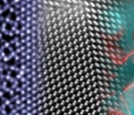
Many of the functional materials we hope to leverage for next-generation technological applications — such as computing, energy harvesting and storage, or communication devices — draw their unique and sometimes exotic properties from a suite of interactions between the atoms, spins, and charges in a crystalline lattice. With direct, real-space access to these order parameters down to the atomic scale, the scanning transmission electron microscope (STEM) is a powerful tool to probe the fundamental framework of such compounds and their properties. As an example of this, I will show how advanced STEM techniques can elucidate key questions about the landscape of superconductivity in recently discovered nickelates. But many of these functional systems are most useful (and therefore interesting) away from the ambient conditions of most typical high-resolution STEM experiments, for instance at cryogenic or elevated temperatures or under an external bias. It is therefore imperative to expand the environmental compatibility of these methods through the parallel development of both hardware and data processing tools, key examples of which will be highlighted here.
[more]