Micro goes Macro
A fully automated, high resolution, large-volume 3-dimensional microstructure characterization system
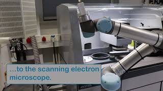
We are standing in a large room with different devices: a high-resolution scanning electron microscope, a sample polishing automaton and a collaborative robotic arm, all embraced by a computer control system. Dr. Shao-Pu Tsai, postdoctoral researcher in the group “Microscopy and Diffraction” places a metallic sample into the polishing machine. The machine adjusts the sample, and then follows a dedicated script to remove an about 1 µm thick layer by a set of different polishing steps. While we are discussing about the possibilities of 3D characterization, the polished and cleaned sample is automatically moved to the transfer station inside the polishing machine where the sample is released from the tight holding in the machine. Then the robotic arm smoothly moves to the polishing machine, takes up the sample and turns to the scanning electron microscope placed next to the polishing machine. The robot opens the analysis chamber of the microscope, puts in the polished sample and closes the chamber again. The microscope immediately starts its own script consisting of pumping, adjusting the sample position, switching on the electron beam, taking electron images of the sample at various magnifications and finally performing a crystallographic and compositional scan across a large surface area. Only a few minutes later a microstructure map of the sample surface appears as a false-colour image on the multiple computer screens placed next to the microscope. After scanning the sample surface, the robot opens the analysis chamber, takes out the sample, closes the chamber and returns to the polishing machine to repeat the whole process. Every polished and scanned surface finally represents one slice in a three dimensional data block which may be as large as 500 × 500 × 500 µm³ measured in steps of 1 µm in every dimension of space.
“This process takes about 15 minutes from placing the sample into the polishing machine, till seeing first results of the scanning process. We are able to analyse 40 slices per day and the whole system works 24 hours without pause. Over a weekend we may collect up to 30 million data points”, explains Tsai. But, why do we need such huge amounts of data? “Before developing this system, we were only able to characterize grain boundaries two-dimensionally and could only guess how they are distributed in the bulk alloy. This system now allows a 3D characterization of grain boundaries and enables us to focus on the interpretation of the data instead of spending time and effort on the polishing and microscopy process.”, states Dr. Stefan Zaefferer, head of the “Microscopy and Diffraction” group. He and his team at the MPIE built up this system, combining commercially available devices with devices made at the mechanical and electronic workshops of the MPIE. “I am especially proud of this in-house cooperation bringing together materials scientists, software developers and various technicians. The software developer who set up the communication between the microscope and the robot, is a newly graduated trainee of us. Our mechanical workshop designed and produced the sample holder for the polishing machine and the microscope, and the electronic workshop designed the communication hardware, necessary to orchestrate all the different devices”, so Zaefferer. Now the scientists are able to analyse the morphology of grain boundaries, seeing for example, which grain boundaries corrode in stainless steel and understanding why this happens and how to prevent the corrosion. A next future step could be connecting this automated system with big data and machine learning programmes developed in the Computational Design department of the MPIE.
