How to design more reliable nano- and micro-electro-mechanical systems
Scientists analyse the deformation behaviour of silicon in nano/micro devices and publish their latest results in PNAS
Mobile phones, data storage for laptops, solar cells, power electronics for renewable energy, or sensors in cars are applications where silicon is the first-choice material despite that its mechanical behaviour at elevated temperature is not yet fully understood. To design efficient and reliable miniaturized devices operating safely with durability at temperatures exceeding room temperature, understanding the deformation mechanisms in silicon becomes crucial. Scientists from the University of Illinois, USA, and the Max-Planck-Institut für Eisenforschung (MPIE), Germany, present insights from sophisticated small-scale mechanical experiments explaining unexpected plastic deformation of silicon on the nanoscale. They published their latest results in the journal PNAS.

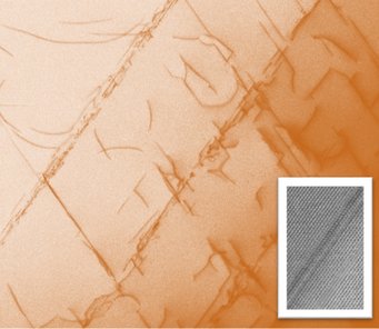
While bulk silicon is brittle at room temperature, it becomes ductile at temperatures of about 540°C and starts to deform easily at about 800°C. The mechanical behaviour of silicon in micro- and nanoscale devices as used in the electronics and sensor industry, is quite different. “In small-scale devices silicon creeps at much lower temperatures of about 400°C depending on the stress level it experiences.”, explains Dr. Mohamed Elhebeary, formerly doctoral researcher at the University of Illinois and now at Intel Corporation. The scientists did in situ bending experiments inside a scanning electron microscope at 400°C, using silicon microbeams. Those microbeams are often included as springs in electro-mechanical sensors. “To be able to do these kind of experiments, we developed in the last years a new in situ thermomechanical lab-on-chip testing set-up. This is how we precisely measured changes in deformation and load with time.”, states Prof. Taher Saif, professor at the University of Illinois. The small size of the silicon beams and the stress achieved through bending, result in a high stress level near the surface of the beam. Transmission electron microscopy studies down to the atomic level were performed at the MPIE in the department “Structure and Nano-/Micromechanics of Materials” by Dr. Tristan Harzer, formerly doctoral researcher at the MPIE and now at JEOL Germany. These studies revealed that the nucleation of dislocations mediates the unexpected plastic deformation of the silicon beams. Thereby, dislocations start to nucleate from the surfaces at the places that experience the highest stress level while bending, and move into the bulk. “What happens when a threshold stress level is reached? We showed that at a certain stress level multiple dislocation nucleation sites appear. With time, as the dislocations spread into the bulk, irreversible deformation occurs until the stress level gets too small to move the dislocations further” states Prof. Gerhard Dehm, director at the MPIE.
The scientists showed that silicon used in nanoelectronics deforms at much lower temperatures than expected. These results are important to design reliable silicon nanodevices operating at high temperatures and stress.
The research was funded by the US-American National Science Foundation.
Author: Yasmin Ahmed Salem
