
Solid state dewetting phenomena of aluminum thin films
Thin films are used in a variety of technologies, e.g. as coatings or for microelectronic applications. Miniaturization and the eventually high surface to volume ratio might enhance thin film degradation. Understanding and controlling of the underlying processes will help to establish reliable and controlled devices or new scopes of application. In this project, we focus on well-defined aluminum thin films as model system and their solid state dewetting behavior.
Thin films are often unstable in the as-deposited state and might undergo massive changes when exposed to high enough temperatures. Besides grain growth, dewetting can occur and eventually lead to an array of particles instead of a dense film. The process is termed solid state dewetting in the case of a temperature below the melting point of the thin film’s material.
In this project epitaxial, highly textured aluminum thin films on single crystalline sapphire (α-Al2O3) substrates serve as model systems. Physical vapour deposition techniques under (ultra) high vacuum conditions are used for thin film deposition. The highly oxophilic Al film is prone to oxidation and forms a few nm-thin native surface oxide which highly impacts the solid state dewetting behavior. Despite preventing the usually dominating surface diffusion, dewetting takes places via grain boundary and interface diffusion. Our studies reveal the formation of voids below a thin surface oxide due to a retraction of the Al thin film. Understanding of the involved processes help to refine solid state dewetting models and thin film degradation.
The current focus of the research project is on the involved mechanisms and dynamics. In-situ annealing experiments are carried out in an environmental scanning electron microscope (ESEM) in oxidizing respectively reducing gas atmosphere. Characterization is carried out before and after the in-situ experiments using various techniques such as secondary electron microscopy (SEM), focused ion beam (FIB), electron backscatter diffraction (EBSD) and different transmission electron microscopy (TEM) methods, like e.g. atomic resolved scanning transmission electron microscopy (STEM), energy-dispersive X-ray spectroscopy (EDX) and electron energy loss spectroscopy (EELS). The complementary methods are used to study the morphology, microstructure and chemistry of the thin film, and the different interfaces (surface|Al thin film and Al thin film|sapphire substrate) or triple phase boundaries and the temperature induced changes.
 Evolution of a faceted void while annealing in an ESEM in oxidizing atmosphere. (b) The cross-sectional color-coded HAADF STEM image reveals a continuous alumina membrane (bright blue) covering both, the void (black) and the film (green). (c) Atomic resolved STEM micrograph of a region adjacent to the Al|void interface (overlay: Al red, O white). (d) EBSD out-of-plane orientation map of a {111} textured Al film (blue) next to a void (red) with twin boundaries in white and further grain/phase boundaries in black.")
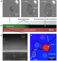
(a) Evolution of a faceted void while annealing in an ESEM in oxidizing atmosphere. (b) The cross-sectional color-coded HAADF STEM image reveals a continuous alumina membrane (bright blue) covering both, the void (black) and the film (green). (c) Atomic resolved STEM micrograph of a region adjacent to the Al|void interface (overlay: Al red, O white). (d) EBSD out-of-plane orientation map of a {111} textured Al film (blue) next to a void (red) with twin boundaries in white and further grain/phase boundaries in black.