Crystal growth simulations of ternary group-III nitride alloys
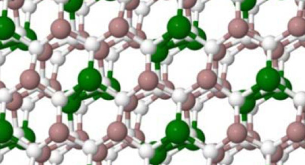
Realization of the direct green light emitting diode (LED) by utilizing GaN based alloys is the next big challenge in solid-state LEDs. A major obstacle is the rather poor material quality of In-rich (exceeding x = 0.3) InxGa1-xN epilayers. To this end, we have developed an effective crystal growth modeling technique in order to elucidate the growth processes of InGaN epilayers on the atomic scale. Our growth simulations reveal a hitherto unexpected √3×√3 pattern in In1/3Ga2/3N epilayer structures.
Realization of the direct green light emitting diode (LED) by utilizing GaN based alloys is the next big challenge in solid-state LEDs and will consequently opens up new applications and markets. Figure 1 illustrates a basic structue of GaN based LEDs. Epitaxially grown InGaN alloys constitute the light emitting part, which is called the active layer. InGaN alloys are currently the most promising candidates for the active layer of efficient green LEDs.

A major obstacle in improving and optimizing green LEDs is the rather poor material quality of In-rich (exceeding x = 0.3) InxGa1-xN epilayers due to the large lattice mismatch (~11%) and thermal stability difference between InN and GaN. An important step to improve the material quality of InGaN epilayers is a detailed understanding of growth processes on atomic scale. While an atomic-level understanding of growth processes derived from experimental methods has thus far remained elusive, a complementary computational effort is indispensable. In fact, a series of ab-initio studies by Neugebauer and coworkers provide important insight into the surface structures and growth kinetics of InGaN.[1-3] However, questions about the atomic-level structure of fully grown InGaN epitaxial layers have yet to be answered, mainly because realistic models of strained InGaN alloy system typically contain a large number of atoms and are cost-prohibitive to address exclusively with ab-initio methods.

The primary focus of our research is to establish practical growth models that enable us to elucidate the growth processes of InGaN epilayers on atomic scale. To this end, we develop an effective crystal growth modeling technique that combines a semi-grand-canonical Monte Carlo simulation with an ab-initio parameterized empirical force field. As illustrated in Fig. 2, this approach enables us to investigate local strain effects on the spatial distribution of In in InGaN epitaxial layers, with particular attention to the effect of surface. Subsequent growth simulations highlight a superstable √3×√3 patterned In1/3Ga2/3N epilayer structure, as shown in Fig. 3

The improved understanding, followed by subsequent theoretical investigations on the interplay between their structural and electrical properties, provides insight into the important factors that determine the optoelectronic properties of InGaN LEDs. This insight will help to identify new routes in solving one of the major obstacles in further improving efficiency in modern solid-state light emitters, from both crystal growth and materials design perspectives.


