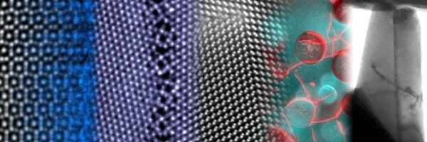
Advanced Transmission Electron Microscopy
The key to establish a fundamental understanding of the links between synthesis, microstructure and properties is to characterize materials on all hierarchical levels of microstructure. Advanced Transmission Electron Microscopy offers versatile techniques enabling the analysis of atomic arrangements, microchemistry, defect structures, interfacial phenomena and precipitate structures. The development and application of advanced TEM techniques, including atomic resolution aberration-corrected imaging, analytical TEM and in-situ TEM are major areas of research.
The research activities of the “Advanced Transmission Electron Microscopy” group revolve around the application and development of advanced transmission electron microscopy (TEM) techniques to study the microstructure, microchemistry, deformation structures and their corresponding evolution in structural and functional materials. The main focus is to establish a fundamental understanding of materials down to the atomic level and to correlate its impact on the materials properties. The area of research includes the investigation of solid-state phase transformation mechanisms, the characterization of interfacial phenomena in precipitation strengthened alloys and microelectronic materials, the phase evolution and interfacial properties in thin film materials, and the nano-mechanical behavior of materials and its related defect structures.
State of the art TEM techniques such as atomic resolution aberration-corrected imaging, high resolution analytical TEM, including energy dispersive X-ray analysis (EDX) and electron energy loss spectroscopy (EELS); as well as in-situ TEM methods are employed to facilitate the length-scale bridging microstructural characterization. The experimental observations are complemented by computational methods to establish guidelines for microstructural design of materials.